Research Description
(On this page I will provide a more detailed description of the research that I performed during the summer)
![]() MENU
MENU
![]() Homepage Research
Progress Summer
REU Activities
Homepage Research
Progress Summer
REU Activities
This
summer our group worked on testing the Token Bit Manager chips that will be
used on the CMS detector. Testing the TBM chips is a matter of patience and
delicacy. The individual chips must be placed on a 3D maneuvering platinum
alloy stage (also called the “chuck”) and loaded into a testing area. Plastic
tweezers are used in tandem with a grounding strap to ensure no electrostatic
discharge that could ruin the TBM. A large testing circuit board is suspended
above the chuck with probes that point downward to a central point. Due to the
TBM’s very small size, a microscope is required to navigate the TBM to make
contact with the testing board. This can prove a tedious process of aligning
and shifting the stage as it is slowly raised, along with the TBM, up to the
probes. Once contact is made the testing process can begin. A simple power box
is turned on to allow a certain voltage to be applied to the TBM through the
test card. Then a software program is run that tests the TBM in various ways.
The program ensures the integrity of data sent through the TBM, as well as the
TBM’s own stability. If the TBM passes this test, a new chip can be prepared
and the current chip cleared on the list. If the test is unsuccessful a number
of variables can be altered to decide if the chip is truly broken, or if the
TBM is merely experiencing bad electrical contact. Occasionally, due to a thin
layer of oxide building up on the chips, the TBM may appear to fail the full
test. This contact error can be overridden through making harder contact;
however, this is not the best option. Many times, shifting the so-called “step
size” of the TBM can absolve the issue as well.
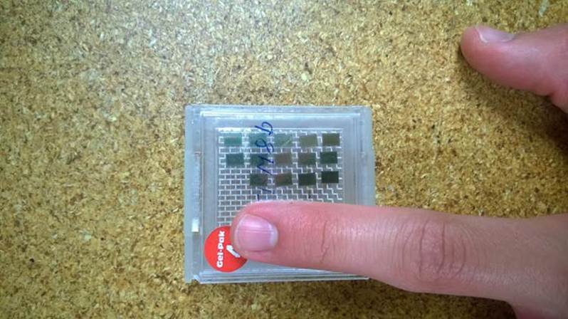
A
bit of perspective on just how small the TBMs are.
The TBM chips work in a unique way. The TBM is designed to work in a sequence that is known as a trigger. Certain triggers are low-level events that occur at low energies and are relatively uninteresting to the physicists at CERN. To flush out these common events the CMS detector has a system of identifying and disregarding such data. The TBM is crucial to mediating such a process. As a low-level event passes through the inner tracking system the TBM chip stores the data from this event. Then, the whole tracking system of the CMS detector identifies the event as uninteresting. Once this process is recognized, the TBM then resets the Read Out Chips (ROCs) attached to itself and clears the data. The TBM also manages the ROCs by sending out what is known as a token. This token goes through all the ROCs that the TBM is managing. If the token returns to the TBM then the data stored in the ROCs gets dumped into the outgoing data stream. This process is known as data acquisition (DAQ). If the token does not return, the event is labeled a “no token pass” and the data from that event is not kept. Through this process, the CMS detector is able to seriously filter the incoming data to a manageable amount.
Testing the TBM Chips
(Testing the TBM chips for functionality)
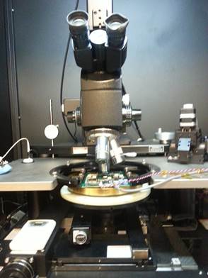
The setup for the TBM chip testing utilized equipment fairly standard for delicate electronics. All tests were carried out in a semi-cleanroom environment to ensure chip integrity and safety. A microscope setup placed onto a Vibraplane ensured that the testing area is not disturbed by random movement during the testing sequences. A Cascade® probe station was used for testing. The hardware was controlled using Nucleus 3.2® software.
The microscope setup for testing TBMs.
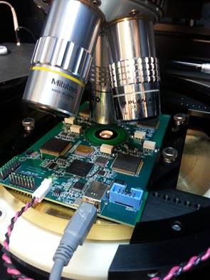
Here is Alex loading one of the TBM wafers into the testing area.
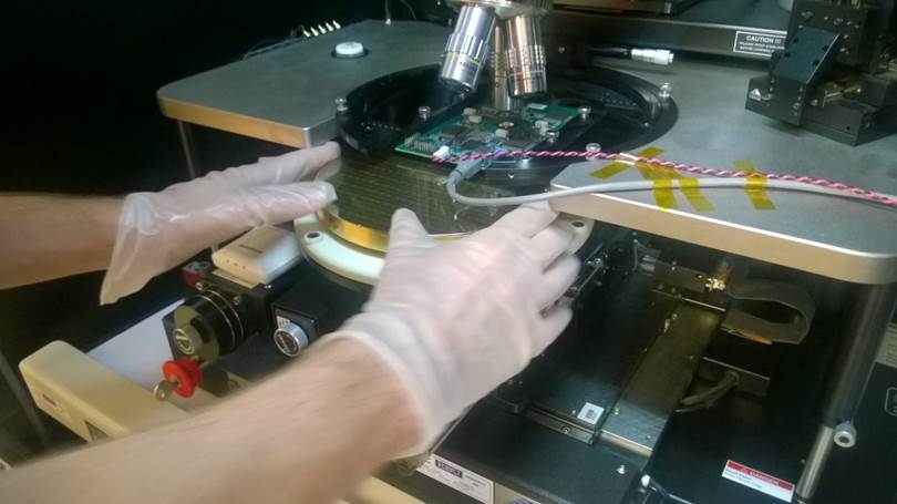
Process: We tested the TBM chips in two waves. First, we were granted a number of pre-sliced individual TBMs to test. These had to be loaded into the testing area one at a time before the test could be carried out. Our second round of testing consisted of using large silicon wafers with thousands of TBM chips on each wafer. These wafers could be loaded onto the testing area and aligned precisely, so the software made testing multiple circuits much easier. The basic process was as follows:
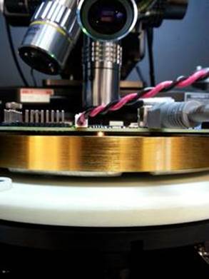
1. The TBM chip (or wafer) was placed on a free moving, but precise, platinum alloy stage.
2. The TBM is aligned using a digital microscope and slowly raised to make contact with a testing board positioned above the stage.
3. Then, the chip makes contact with the probes on the testing
board (this could be confirmed through small scratches on the TBM contact
pads).
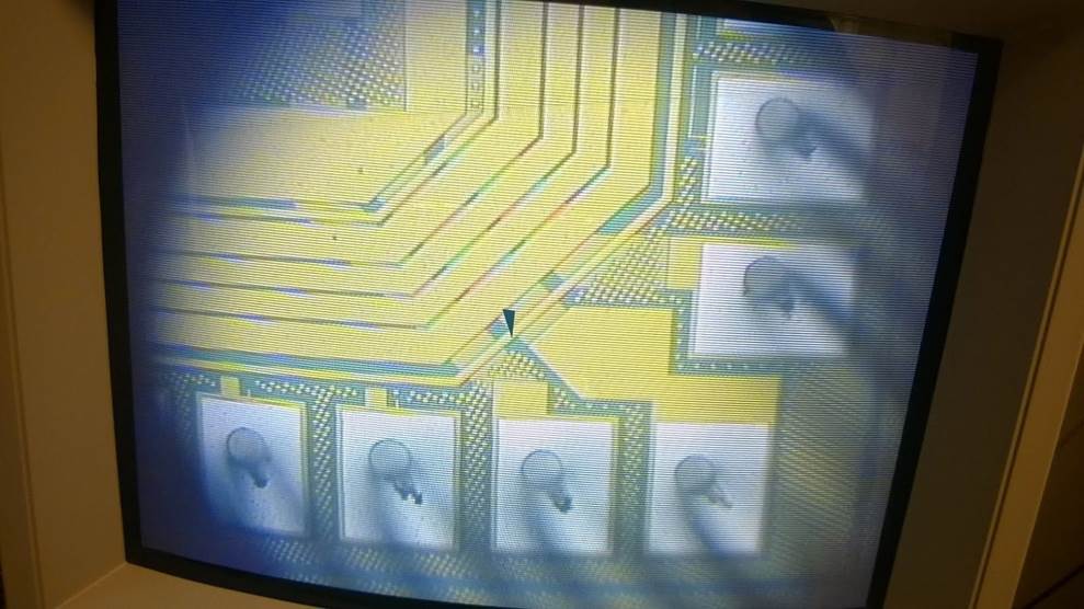
This
monitor displays the microscope’s view of the contact probes. We use it to navigate
and align the probes to connect with the TBM contact pads. Once contact is
achieved, one can see the slight scratch marks indicating a touchdown from the
probes.
4. Voltage is then supplied to the TBM.
5. Tests are run using a code developed by post doctorate students at KSU. The test code assesses a TBM’s highest operating frequency along with many other features.
6. TBM test results are then exported via XML format.
Results: All of the TBM chips that we managed to test passed the minimum requirements that deem them functioning. Many of the chips surpassed the 40 MHz benchmark set for them; some TBMs even passed the testing at 50 MHz or higher. Even so, some TBMs were not quite as functional, and they were only able to function at the minimum requirement of 40 MHz.