Testing New Instrumentation for the Phase-2 CMS Detector Upgrade
Nat Penn, Boston University, Physics and Music Composition (dual degree)
Mentored by Dr. Andrew Ivanov
Introduction and Methods
The field of high-energy physics (HEP) aims to study the fundamental particles and forces that make up the universe around us. One way to study this is by using particle colliders, which accelerate bunches of particles using electromagnetic fields then cross the paths of the particle beams so they collide at high speeds, then measure the output particles. The Large Hadron Collider (LHC) is the world’s largest particle accelerator at 17 miles in circumference and is located near Geneva, Switzerland. It is a ring collider which uses beams made of proton bunches. Experiments performed at the LHC led to the discovery of the Higgs boson in 2012, a particle that is very important to physics but was previously only theorized. The LHC currently runs at 6.8 TeV per beam and up to 13.6 TeV collision energy and is currently preparing for the installation of the high-luminosity (HL) upgrade, which increases luminosity (the collision rate of particles in a given cross-sectional area) by a factor of 5-10 to improve measurements and increase chances of new particle discovery.
The Compact Muon Solenoid (CMS) detector is one of the two major detectors (the other is ATLAS) in the LHC. The innermost layer is the tracker, which is made of approximately 13,000 silicone chips whose pixels detect “hits” when particles pass through them then quickly process, store, and send this data. This data is then used to measure and analyze the momentum of particles by detecting when particles pass through pixels in different locations. Part of the HL-LHC phase 2 upgrade involves testing then implementing improved RD53 chips (known as CROC or CMS Read Out Chips) which have a higher pixel density and radiation tolerance. At the point of writing this article, RD53B CROC-v2 chips are being tested at Kansas State University and University of Turin in the form of wafers. Wafers are flat disks of silicone with 136 chips each that facilitate faster testing due to the ability to automate testing of multiple chips in succession rather than individually. 55 wafers are to be tested at Kansas State University.
Wafers are tested at Kansas State University (KSU) on an MPI TS-3000 probe station. The operators of the machine align the wafer using the digital microscope then run the wafer testing python script. During testing, around 200 probe tips (extremely fine tungsten needles mounted on a probe card) make contact with landing pads on each chip and run around 25 tests to ensure qualities like chip functionality, pixel functionality, digital logic, data processing, and contact resistance are working properly.
After this, operators run a wafer analyzer python script on the output log file, which generates a PDF file that includes data about the wafer’s performance on each test. This also includes a general “wafer map” which displays the status (represented by green, yellow, red, and gray) of each chip in a graph representative of the chip locations on the wafer. Additionally, it produces json files for each wafer and each chip on the wafer. KSU researchers in the summer of 2024 have been developing new scripts to analyze the wafer testing results, like contact resistance over time and by chip, number and type of errors, contact resistance compared with number of errors, maps of the measured contact height and probe tip symmetry, comparisons of multiple wafers, as well as scripts to facilitate monitoring and running of tests. This data is used to improve quality of testing and provide information about what to upgrade for the RD53C (final version) chips.
In June, our probe card (the device on which the probe tips are mounted that communicates between the chip and other equipment) broke, so we had to get a replacement probe card. Therefore, much of the data is based around comparing the yields and errors of the wafers tested with the two probe cards.
Results
The topography and asymmetry maps display the contact height and contact asymmetry for each chip on the wafer, respectively. Contact height is the height in μm at which the chuck makes contact with the probe tips. Asymmetry is the difference in μm between the heights of the two edge sensors, located on either end of the row of probe tips. Generally, lower differences in contact height between chips and asymmetries closer to 0 are better. The topography and asymmetry maps show that the contact resistance and asymmetry do have some correlation with the location of the chip on the wafer. [Fig. 1-4]
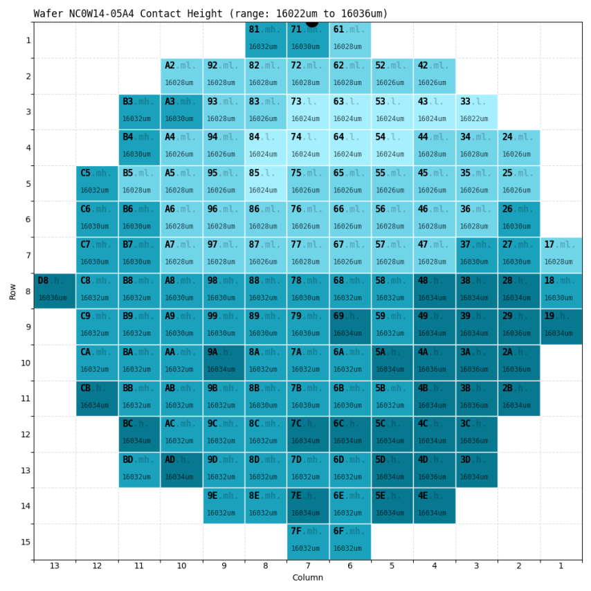
Fig. 1. Topography map of wafer 05A4 (1st probe card)
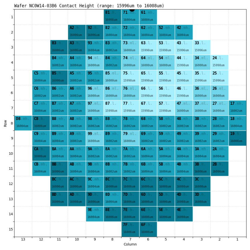
Fig. 2. Topography map of wafer 03B6 (2nd probe card)
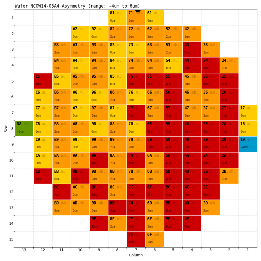
Fig. 3. Asymmetry map of wafer 05A4 (1st probe card)
")
Fig. 4. Asymmetry map of wafer 03B6 (2nd probe card)
Contact resistance is the electrical resistance, in ohms, measured through both digital and analog sections of the chip, when the probe tips make contact with the chip. Generally, a lower contact resistance is better because it is associated with a smaller number of errors. We measure contact resistance of each chip to verify our connection between the probe card and chip. This ensures we have fewer false errors, and increases the accuracy of our tests. In the plots below, it is clear that regular probe tip cleanings do improve the contact resistance, and cleanings spaced to be every 20 chips are sufficient to keep the contact resistance at appropriate levels. [Fig 5-6]
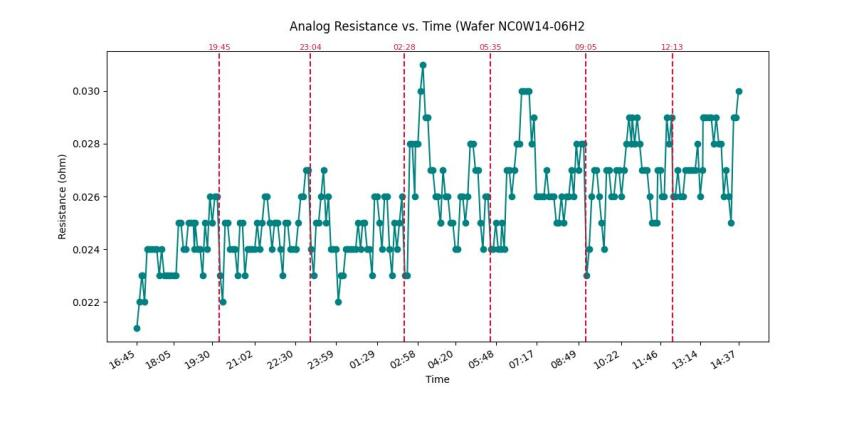
Fig. 5. Analog resistance for wafer 06H2 over time with vertical lines representing cleaning times
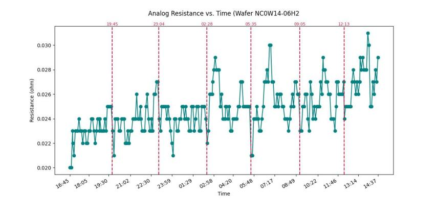
Fig. 6. Digital resistance for wafer 06H2 over time with vertical lines representing cleaning times
Another crucial part of wafer testing is error monitoring and analysis. When the wafer is analyzed, chips are marked as red (failed essential tests), yellow (failed non-essential tests), green (did not fail), or gray (did not fully test), and if they are red or gray, a failure reason is assigned to the chip. The failure reason variable is labeled as whichever test or error caused the chip to fail. The plots below are bar plots with each test that caused a chip to fail and the number of chips that failed due to that test. It is important to note that the first probe card only tested two wafers but the second tested three. In these plots, we can see that both had high numbers of scan chain, digital scan, and dead pixels errors, but the 2nd probe card had significantly more DAQ digital scan errors. However, there were several tests that appeared on the first probe card that were not on the second. With more data we will be able to perform deeper analysis on the errors given by the unsuccessful chips and have a better understanding of what kinds of issues might occur within the detector and updates to make to future models. [Fig. 7-8]
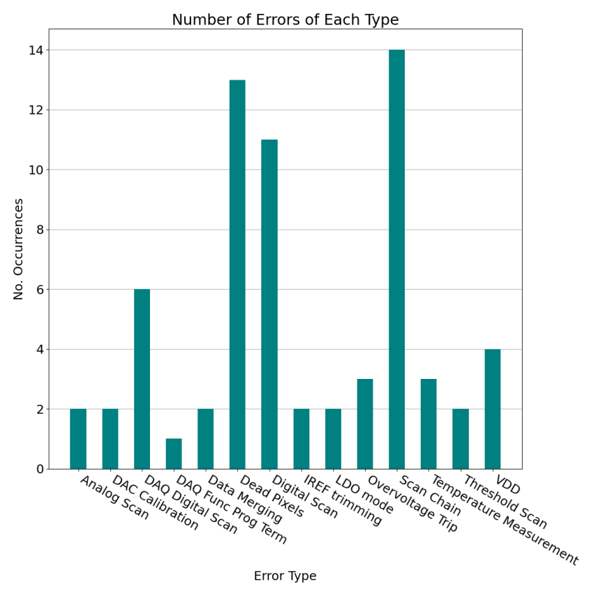
Fig. 7. Failure reasons for 1st probe card (2 wafers)
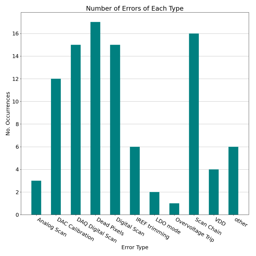
Fig. 8. Failure reasons for 2nd probe card (3 wafers)
As of 08/2/2024, only 11 wafers have been tested at Kansas State University. As more wafers are tested, we will get more data and can use this data to understand more about the functionality of the CROC-v2 chips. Conclusions from these tests will contribute to the further development and eventual implementation of the new instrumentation for the HL-LHC CMS upgrade.
Acknowledgments and Sources
Special thanks to: Andrew Ivanov and Wyatt Jones (Kansas State University); Matt Bellis, Julie Hogan, Sal Rappoccio, Anders Ryd, and Steve Cullen (USCMS MREFC EPO Internship Program); the CERN team, especially those working on the CMS detector, and other members of the CMS collaboration. This program is funded by the National Science Foundation (NSF) grant number 2310056. Any opinions, findings, and conclusions or recommendations expressed in this material are those of the author(s) and do not necessarily reflect the views of the NSF.
[1] CMS’ High Luminosity Tracker Chip Is Ready! | CMS Experiment, in (n.d.).
[2] Herr and B. Muratori, Concept of Luminosity, (n.d.).
[3] Schwartz, ContactResistanceAnalog, (n.d.).
[4] Grippo, Croc_wlt, (2021).
[5] Detector, https://cms.cern/index.php/detector.
[6] Apollinari, Béjar Alonso I, Brüning O, Lamont M, and Rossi L, High-Luminosity Large Hadron Collider (HL-LHC) Preliminary Design Report.
[7] Moreira, lpGBT Project Status and Plans, https://indico.cern.ch/event/863071/contributions/3738814/attachments/2044931/3425692/lpGBTstatusAndPlansACES20200526.pdf.
[8] LS3 Schedule Change, https://hilumilhc.web.cern.ch/article/ls3-schedule-change.
[9] Grippo and F. Luongo, Phase 2 Pixel Upgrade CROC Wafers for CMS Experiment, (2024).
[10] Christiansen, RD53 Pixel Readout Integrated Circuits for ATLAS and CMS HL-LHC Upgrades.
[11] Christiansen and RD53 collaboration, RD53B Users Guide: Introduction to RD53B Pixel Chip Architecture, Features and Recommendations for Use in Pixel Detector Systems., (2021).
[12] M. Sirunyan et al., Search for Vectorlike Light-Flavor Quark Partners in Proton-Proton Collisions at s = 8 TeV, Phys. Rev. D 97, 36 (2018).
[13] Grippo, Summary of the CROC WLT Review, (unpublished).
[14] The Floating CMS | CMS Experiment, https://cmsexperiment.web.cern.ch/news/floating-cms.
[15] The RD53C-CMS Pixel Readout Chip Manual, (2024).
[16] TS3 000-SE, https://www.atv-systems.com/mpi-wafer-test-systems/mpi-automated-systems/ts3000-se.
Nat Penn CMS Wafer Testing Code
Final Presentation