III Nitride Semiconductor Research
by Thomas Erickson
supervisor: Dr. Lin
Kansas State University Physics Department REU Program, sponsored by NSF
Welcome to my webpage. I’m working with the III Nitride semiconductor group at KSU over the summer of 2007. Currently I am working on getting our NSOM machine back in commission so they can use it. This primarily involves finding out how our NSOM machine works, and then using it carefully enough not to break it.
Below I describe My Research and include some Useful Links.
Also check out my final presentation
NSOM stands for Near-field Scanning Optical Microscopy. It involves using a very fine (~50 nm) fiber optic tip, coated with reflective metal, that is held very close (~1-2 nm) to the surface of a sample. From here it is used to gather light. By getting so close to the material you’re studying, you can surpass the diffraction limit of the light, and resolve images on the order of the fiber optic tip. The tip is also used as an Atomic Force Microscope, which basically works by tapping the surface to see how far away it is. This gives a combined picture of the optical properties of the local areas of a surface as well as the shape. This is useful to us because a lot of what we’re doing with the semiconductors has to do with their optical properties.
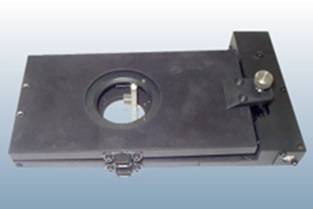
This is the NSOM 2000 TS that I’m working with (Nanonics Ltd.)
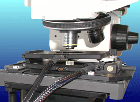
I am working with a NSOM 2000, made by Nanonics Ltd. The system was working previously but has not been used for years. The grad student who had been using it, Jagat Shakya, has left, and no one is currently familiar with the machine. My goal is to get the machine working again, and to then take pictures of semiconductor devices and crystals. The NSOM has 2 parts, the top part that holds the probe and the bottom part that holds the sample. Both are capable of moving relative to one another.
For a day by day summary of what I did, click here
Here are pretty AFM and optical microscope pictures I took. These are just a bunch of wires on a random circuit board we had. The plan is to compare this picture from our working AFM to images from the NSOM machine to make sure the NSOM is working properly.
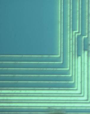
< - - AFM - - - - - Optical - - >
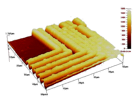
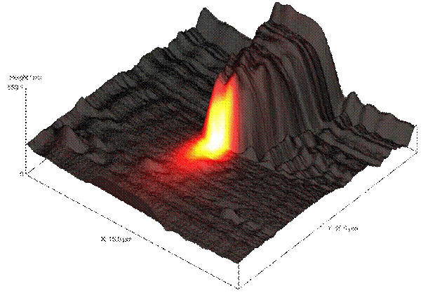
Eventually I hope to take pictures like this one that Jagat took of a waveguide. The shape is the AFM picture, while the color is from the NSOM image. Notice how you can see the light coming out of the end of the optical waveguide.
My Results:
After much work and effort, I was able to get the NSOM machine working, and wrote up a summary of how it works for the lab, so they can use it too. It isn’t working perfectly, but it seems to do roughly what we had hoped it could do. The group is going to eventually take images of photonic crystals, waveguides, as well as characterizing imperfections in their grown semiconductors.
This is a NSOM picture that I took with the machine of a GaN crystal with defects
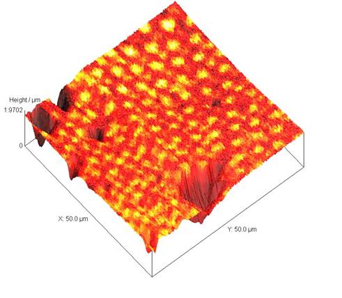
Notice the patterns of light spots and dark spots, but with no lumps on the surface itself. That’s NSOM
Here is a copy of my Final Presentation
Here is an artistic interpretation
for the other REU projects
Check out these useful sites: