8/23/02 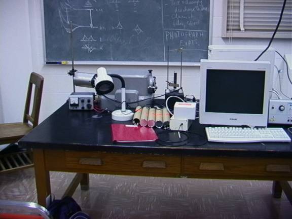 clc
clc
Visible Light Spectra
In this experiment you will analyze the light emitted by simple radiating systems and learn how visible light monochromators/spectrometers operate. Your actual data will be taken using a StellarNet PC based spectometer which uses a grating to disperse light over the range 250-850 nm onto a photodiode array. The data taking and display is done automatically by the software provided with the spectrometer, saving you a lot of work and making the recording of spectra very fast and efficient. However , before using this device, you are expected to examine the operation of a classical MacPherson UV monochromator and understand the principles of its operation.
The descriptions below are very brief. You will probably have to read further to understand and appreciate the experiments. Melissinos, pp. 28-52 is very useful. Atomic energy level tables by Moore are available in the lab. for identifying energy levels. A supplement on determining Planck’s constant with LEDs is provided.
The apparatus includes:
- MacPherson model 218 UV monochromator.
- StellarNet PC based spectrometer and associated software.
- Various discharge tubes (hydrogen, mercury, neon, nitrogen, sodium, etc. )and necessary voltage supply (BE CAREFUL: the supply voltage of 5 kV is potentially lethal).
Supplementary documents include:
- StellarNet Manual
- Writeup on determining h using LEDs
Experiment
1. Monochromator operation: Open the MacPherson UV monochromator and examine the optics inside. The major components of this instrument are the entrance and exit slits, two concave mirrors and a plane grating. Monochromatic light emerging from the entrance slit will be focused at infinity by the first concave mirror. It then is reflected from the grating at an angle determined by the constructive interference requirement. Make a drawing of the optics of the instrument and be sure you understand how it works. Derive the condition for constructive interference in terms of the angles of incidence and reflection from this grating. Note that these angles do not have to be equal: the grating is not a mirror. Upon reflection from the grating, the light is refocused onto the exit slits. As the angle of the grating is scanned, different wavelengths are sent onto this slit. Try to derive the expression for the dispersion of the instrument, defined as dx/dl, where x is the lateral distance across the exit slit and l the wavelength of the light. What determines the wavelength resolution of this instrument?
2. The StellarNet PC based spectrometer:
a. Playing around: Record spectra from various sources in the room, such as the fluorescent lights, light from the sky, light reflected from various objects, light from the computer screen, light from an incandescent light bulb, etc. Explain as many general features of the spectra as you can in your writeup. Quantative analyses are not necessary at this point. Just explain the general characteristics of each spectrum.
b. The hydrogen spectrum: Record the spectrum from a hydrogen discharge tube. Determine the wavelengths of (most of ) the lines, and identify which transitions they correspond to. Construct an energy level diagram for atomic hydrogen and label the transitions you are able to see. Use spectroscopic notation. You may find Melissinos, pp. 28-37 to be helpful. From your data, derive a value for the Rydberg constant.
c. Na spectrum: Record the spectrum from the Na lamp. Find the wavelengths. Using the Moore tables (provided in the lab. room) or some other source, identify all the lines. Construct an energy level diagram for Na and identify which lines you see. Na has one electron outside a closed (Ne-like) core, and thus has many similarities in its level scheme to hydrogen. In your writeup you should discuss these similarities and differences. Be sure you are familiar with the quantum numbers n,l,s and j used in labeling the states. Why are some transitions strong and others weak? What selection rules operate for electromagnetic transitions?
d. Hg spectrum: Record the Hg spectrum from a discharge tube. Identify the strongest lines and construct an energy level diagram. This is a “2 electron” spectrum. What does that mean? What quantum numbers are used to label the levels , and what do they mean?
e. Molecular spectra: Observe spectra from N2, H2O and CO2. How do these spectra differ from the atomic spectra studied above? Why?
e. LED’s and Planck’s constant: You are provided with a number of LEDs. These are solid state devices, diodes, which emit light when voltage exceeding a certain threshold is applied in the forward direction. Roughly speaking, the threshold voltage required is equal to the band gap of the material being used. Using this approximation, record the threshold voltage for each of the LEDs provided, and use the spectrometer to determine the wavelength of the corresponding light emitted. Make a plot of threshold voltage versus 1/ l and use this to determine Planck’s constant.
Using
Light Emitting Diodes (LEDs) to Measure Planck’s Constant
The energy of the photon, E, and its frequency, n, are simply related
E=h n
where h is Planck’s constant. The goal of this experiment is to demonstrate this relation, and to determine the numerical value of Planck’s constant, h, by studying properties of light emitting diodes (LEDs).
LEDs are semiconductor devices that emit light, but
require very little electric power.
LEDs are most often used as ON/OFF indicator lights in electrical appliances
such as televisions and stereos. They
are also used to display the numbers in some alarm clocks, radios, and
microwave ovens. LEDs can be bundled
together to make up a variety of large lights and screens, including traffic
signals, “neon” billboards and sports stadium screens. For example, the large
flat panel displays used on large buildings and stadiums are made up of a
massive number of discrete LEDs. They
are very
energy-efficient light sources. LEDs emit little heat and have long lifetimes.
By comparison, a 15-watt LED stoplight can last, on the average, 20,000 hours,
while a 100-watt house light bulb lasts only about 1,000 hours.
A
simple LED is a semiconductor chip which consists of two different types
semiconductors that have been joined.
The semiconductor with excess negative charge (electrons) is called the
n-type semiconductor. The other
semiconductor, with deficiency of electrons called p-type. So a simple LED is a semiconductor p-n
junction operating under a forward bias condition. In the following, we will present a brief description of the
basic physics of a p-n junction and the condition of the so-called “forward
bais.”
P-n junction under zero bias (under
equilibrium)
Let us consider separate regions of p- and n-type
semiconductor material, brought together to form a junction (Fig. 1) This is
not a practical way of forming a device, but this “thought experiment” does
allow us to discover the requirements of equilibrium at a junction. Before they
are joined, the n material has a large concentration of electrons and a few
holes (or points with deficiency of electrons), where as the converse is true
for the p material. Upon joining the two regions we expect diffusion of
carriers to take place because of the large carrier concentration gradients at
the junction. Thus holes diffuse from p side to the n side, and the electrons
diffuse from n to p. The resulting diffusion current cannot build up
indefinitely, however, because an opposing electric field is created at the
junction (Fig. 1b).
If we consider that the electrons diffusing from n
to p leave behind uncompensated donor ions (Nd+) in the n
material, and holes leaving the p region leave behind uncompensated acceptors
(Na-), it is easy to visualize the development of a
region of positive space charge near the n side of the junction and negative
near the p type. The resulting electric field is directed from the positive
charge towards the negative charge. Thus E is in the direction opposite to that
of diffusion current for each type of carrier (recall electron current is
opposite to the direction of electron flow). Therefore the field creates a
drift component of current from n to p (carried by electrons thermally excited
across the energy gap into the conduction band), opposing the diffusion current
(Fig 1c). Under equilibrium, no net current can flow across the junction and
the current due to the drift of carriers in the E field must exactly cancel the
diffusion current. Furthermore, since there can be no net buildup of electrons
or holes on either side as a function of type, the drift and diffusion currents
must cancel for each type of carrier.
Figure 1
Properties of an equilibrium p-n junction: (a) isolated, neutral
regions of p-type and n-type material and energy bands for the isolated
regions; (b) junction, showing space charge in the transition region W, the
resulting electric field e and contact potential V0, and the separation
of the energy bands; (c) directions of the four components of the charge
flow within the transition region, and the resulting current directions.

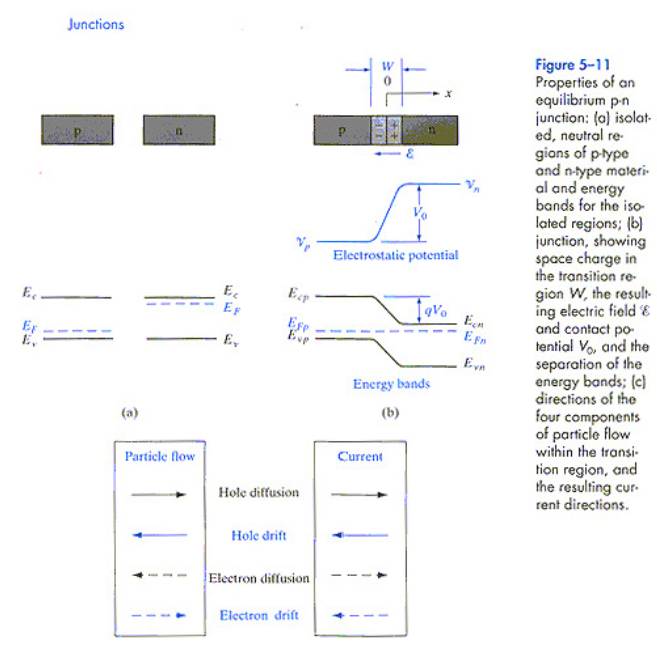
Therefore the electric field E builds up to the
point where the net current is zero at equilibrium. The electric field appears
in some region W about the junction, and there is an equilibrium potential
difference V0 across W. Thus
there is a constant potential difference V0 = Vn - Vp
between the two. The region W is called the transition region, and
the potential difference V0 is called the contact potential or the
built-in potential. The V0 for which the net current becomes zero is
approximately equal to the energy gap, since the Fermi levels on the p and n
sides of the barrier are very close to the bottom of the conduction band and
top of the valence band, respectively.
Qualitative
Description of a p-n Junction Under Biased Conditions
Since an applied voltage changes the electrostatic
potential barrier and thus the electric field within the transition region, we
would expect changes in the various components of current at the junction (Fig
2). The electrostatic potential barrier
at the junction is lowered by a forward bias Vf from the equilibrium
contact potential V0 to the smaller value V0 – Vf.
This lowering of the potential barrier occurs because a forward bias (p
positive with respect to n) raises the electrostatic potential on the p side
relative to the n side. For a reverse bias (V = -V) the opposite occurs; the
electrostatic potential of the p side is depressed relative to the n side, and
the potential barrier at the junction becomes
larger (V0 + Vr). Referring to the electrons, the diffusion
current is very sensitive to the applied voltage because it is carried by those
electrons (on the n side) whose energy , in the Boltzmann distribution in the
conduction band, exceeds the energy step across the barrier. The drift current,
on the other hand, is more or less fixed, limited by the number of electrons
which have exceeded the energy gap into the conduction band (on the p
side). Thus the current will rise
rapidly with voltage in the forward direction, but will quickly saturate at a
small value (the drift current) when the voltage is in the backward direction.
The forward current will increase with voltage until it becomes approximately
equal to the energy gap. At roughly this point, even electrons lying at the
bottom of the conduction band on the n side can flow freely across the barrier,
and the diode current increases very rapidly. This is the turn-on voltage of
the diode, Vo , and occurs roughly for an applied voltage equal to
the energy gap.
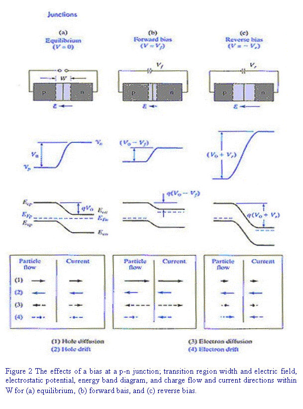
Figure 2
Effects of a bias at a p-n junction; transition region width and electric
field, electrostatic potential, energy band diagram, and charge flow and
current directions within W for (a) equilibrium, (b) forward bais, and (c)
reverse bias.
|
Figure 2
Effects of a bias at a p-n junction; transition region width and electric
field, electrostatic potential, energy band diagram, and charge flow and
current directions within W for (a) equilibrium, (b) forward bais, and (c)
reverse bias. |
Light Emission
In order for the LED to emit light, the electrons
must flow from the n-side to recombine with the hole in the p-side across the
boundary. In order for this current to
be large, a minimum forward bias, Vf, must be applied across the p-n
junction of the LED. To the first order
approximation and assuming perfect Ohmic contacts on p- and n-type materials,
the minimum value of Vf required for any significant light emission
to occur is approximately V0, which is called the turn-on voltage
(or cut-off voltage). The minimum
energy (per one electron) necessary for the current to flow is then eV0. This amount of energy is approximately equal
to the magnitude of the energy gap between the conduction and valence
bands of the material and the emitted photon energy is approximately equal to
the energy gap,
![]()
A
transparent resin that protects the LED from any damage surrounds the LED chip,
shown in Figure 3. In addition, the
resin and a reflector dish found at the base of the chip focuses the emitted
light through the top of the LED.
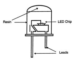
Figure
3. Schematic diagram of an LED.
Using semiconductors with different bandgap energies in LEDs
can control the color of the light emitted by LEDs. The red or green are the most common, but other colors like
orange, yellow, blue, as well as infrared, are available.
Connect the following circuit:
|
Connect the following circuit: |
Experiment
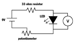
Apparatus:
- several LEDs with different
emission colors
- infrared sensor card
- voltmeter
- 9 V battery and pot, or
variable V supply
- 33
 resistor (please
do not skip this.)
resistor (please
do not skip this.) - breadboard, cables
Presentation
of your results:
Prepare
a plot of photon energy as a function of photon frequency (shown below) and use
it to discuss your results and to determine the Planck’s constant.